Boise State University has developed a new method for manufacturing flexible hybrid circuits.
The school's researchers say it's cheaper, waste-reducing, and eco-conscious compared to traditional techniques. Using laser-induced graphene (LIG), the innovative approach could transform modern electronic production.
Printed circuit boards (PCBs) are the backbone of most electronic devices. Conventional PCB manufacturing often involves harsh chemicals and generates significant material waste. Electronics are also getting smaller and more intricate in the form of wearable technology.
As a result, the demand for flexible PCBs (f-PCBs) is booming. This growing need necessitates more sustainable manufacturing methods.
As Tech Xplore shared, the Boise State team's solution centered on LIG. The laser converts carbon-rich materials into a 3D conductive structure. The procedure is scalable, cost-effective, and allows for precise patterning.
Researchers embedded palladium (Pd) nanoparticles into a polymer matrix to form Pd-functionalized LIG. Nanoparticles create the electroless deposition of copper (Cu) on the LIG scaffold. Then, conductive Cu-pathways take shape for the flexible circuits.
Save $10,000 on solar panels without even sharing your phone number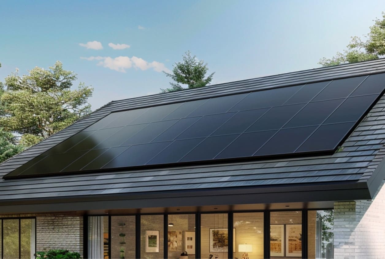 Want to go solar but not sure who to trust? EnergySage has your back with free and transparent quotes from fully vetted providers that can help you save as much as $10k on installation. To get started, just answer a few questions about your home — no phone number required. Within a day or two, EnergySage will email you the best local options for your needs, and their expert advisers can help you compare quotes and pick a winner. |

Laser-based additive manufacturing builds up the circuit layer instead of removing unwanted material.
This new method offers several major advantages.
"Additive manufacturing of printed circuit boards can help advance electronics manufacturing by reducing waste, cutting costs, and enabling rapid prototyping," said Attila Rektor, lead author of the study. "Our approach helps eliminate harmful chemicals and excessive material waste, to help make PCB fabrication more environmentally sustainable."
This is a big deal for an industry valued at around $90 billion globally. Reducing chemical use and material waste protects the environment while increasing the reusability of electronics.
TCD Picks » Quince Spotlight
💡These best-sellers from Quince deliver affordable, sustainable luxury for all


|
Which of these factors is the biggest obstacle preventing you from getting solar panels? Click your choice to see results and speak your mind. |
Consumers get the benefit of more affordable and innovative flexible electronic devices. Smartwatches, for example, give access to new modes for health and wellness tracking. For companies, it offers a path to greener production methods such as solar.
"[Rektor's] research not only bridges fundamental scientific discovery to practical applications but also introduces an innovative approach to manufacturing flexible PCBs — reducing costs and environmental impact by eliminating waste and harmful etching processes for our industrial partners," said professor David Estrada from Boise State's Micron School of Materials Science and Engineering.
The university's pivotal research is the start of a sustainable, efficient future for electronics manufacturing.

Join our free newsletter for weekly updates on the latest innovations improving our lives and shaping our future, and don't miss this cool list of easy ways to help yourself while helping the planet.